Smart New Energy Solutions
供应链管理经验丰富:创始人拥有 20 年 + 的电子行业供应链管理经验,能精准把控供应链运作。
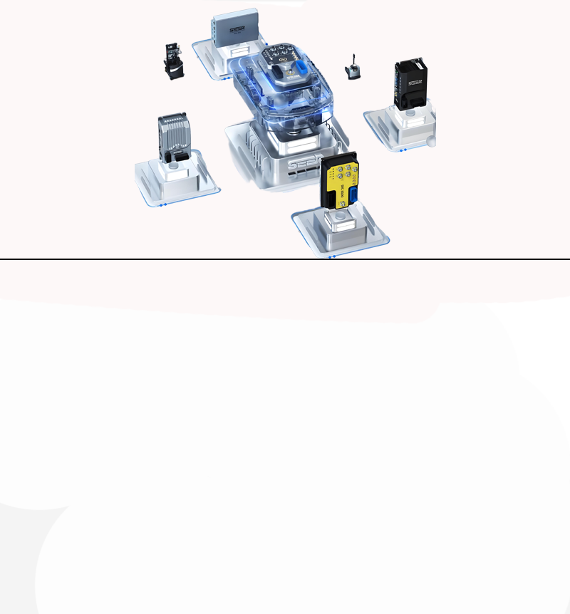
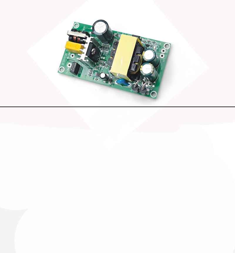
模块化产品设计:可为客户提供高效的模块化智能连接方案,精选优质的国内外电子元器件。
高效的工程师团队:拥有一支完整的产品工程师团队,能够快速匹配客户需求并开发产品。


这篇文章主要介绍了汽车电池管理系统(BMS)中二次监测系统的作用及其优势,并重点推荐了ABLIC的汽车电池保护IC作为二次监测的理想解决方案。
智能手表,智能家居,扫地机器人,物联网(IoT)智能家居
智能小家电控制系统,AI 语音交互厨房电器,2025 年智能家电互联互通,模块化设计家电
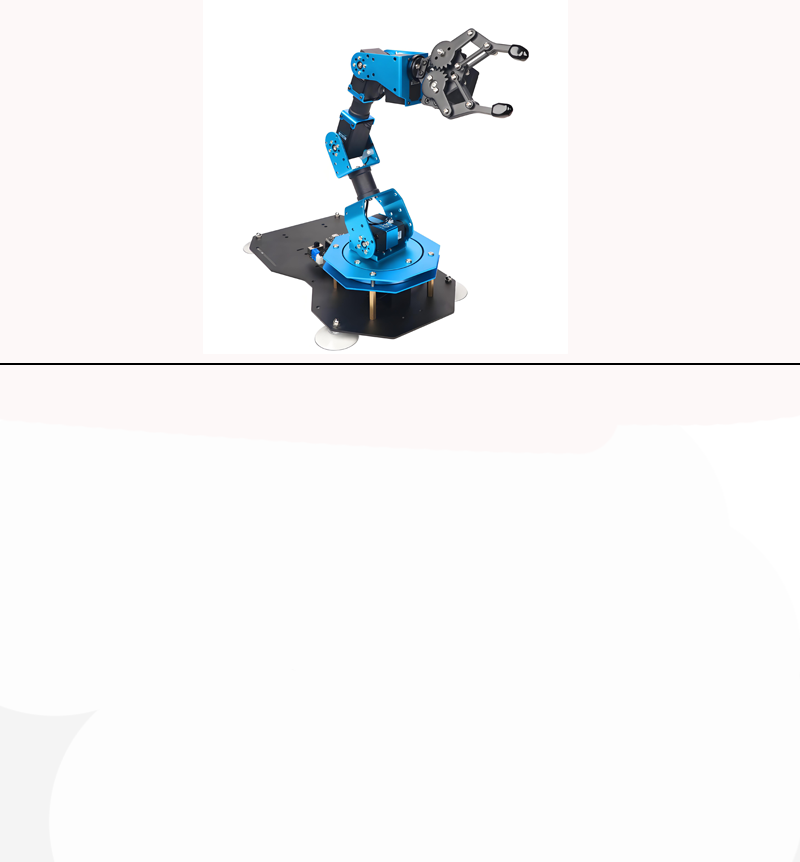
客户背景 客户是国内一家专注于具身智能工业机器人研发的高新技术企业 核心挑战 技术壁垒:工业场景中要求毫秒级响应,需优化硬件架构设计(如多核处理器调度)及算法轻量化; 性能匹配:工业控制领域,满足工业设备对实时性和稳定性的需求…
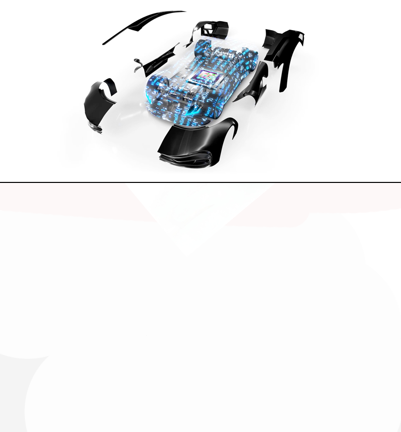
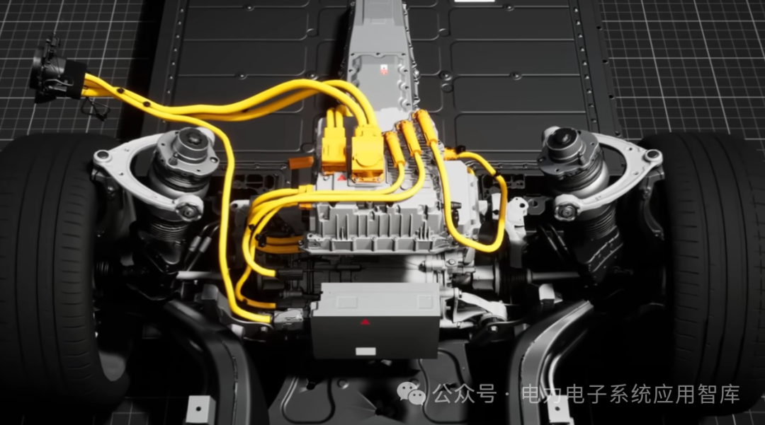
芯湃科技助力某自主品牌高端电动轿车实现核心硬件85%国产化替代,突破车规级SiC电驱、高精度BMS芯片等“卡脖子”技术,搭载自研ASIL-D级MCU芯片及国产操作系统,打造全栈本土化硬件生态。方案覆盖电驱、电池管理、域控制器等关键模块
PLC,工业机器人控制,智能制造,汽车制造工业控制
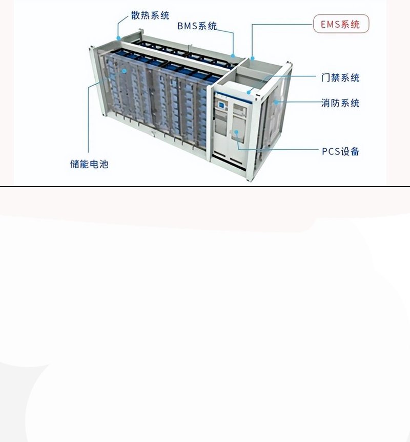
储能变流器(PCS),电池管理系统(BMS),新能源配储政策,bms
客户背景 某国内电源生产品牌为适应国内市场所带来的冲击,希望通过推进国产化芯片来进一步降低其产品生产成本,同时通过降低供应链交货周期缩短备货周期。 核心挑战 技术壁垒:高精度电源管理芯片、can隔离芯片等长期被TI、NXP及企业垄断; …
新能源汽车智能悬架技术不断迭代创新发展,主流车企在汽车悬架技术层面先后展示过蔚来香槟塔不倒,仰望U7车顶咏春平稳挑战,华为尊界白沙不扬,玻璃不碎,踏水无痕等各种不同悬架技术,这些悬架功能的实现依赖于对悬架中弹簧和减振器的调节得以实现,在悬架系统的构…


安森美 48V 汽车平台的完整解决方案体系,系统拆解其在汽车电气化进程中的战略定位与核心价值,深入剖析功率模块集成、MOSFET 技术迭代、散热封装创新等关键技术突破,详细梳理了涵盖功率器件、保护器件、驱动控制等全链路的核心产品组合,并针对 48V-LV DC-DC 转换…
电动汽车向高电压、高集成度与智能化发展过程中,48V区域化电源分配网络(PDN)成为技术突破关键。该系统通过高密度GaN/SiC电源模块(功率密度提升3倍)、动态功率分配及模块化设计,解决了系统复杂性、充电兼容性、轻量化等挑战。区域化架构缩短线束60%,减重18kg,…

随着汽车电动化、智能化浪潮推进,48V 轻混系统已成为降低油耗、提升动力性能的核心方案之一。高边开关芯片作为 48V 系统中负载驱动、电源分配的关键器件,其性能、可靠性直接影响整车运行安全与效率。目前全球市场呈现国际厂商主导、国产加速追赶的格局,本文从市场…
藏芯于微,智启未来